- 您现在的位置:买卖IC网 > Sheet目录501 > QEE123E3R0 (Fairchild Optoelectronics Group)LED IR ALGAAS SIDELOOK 880NM
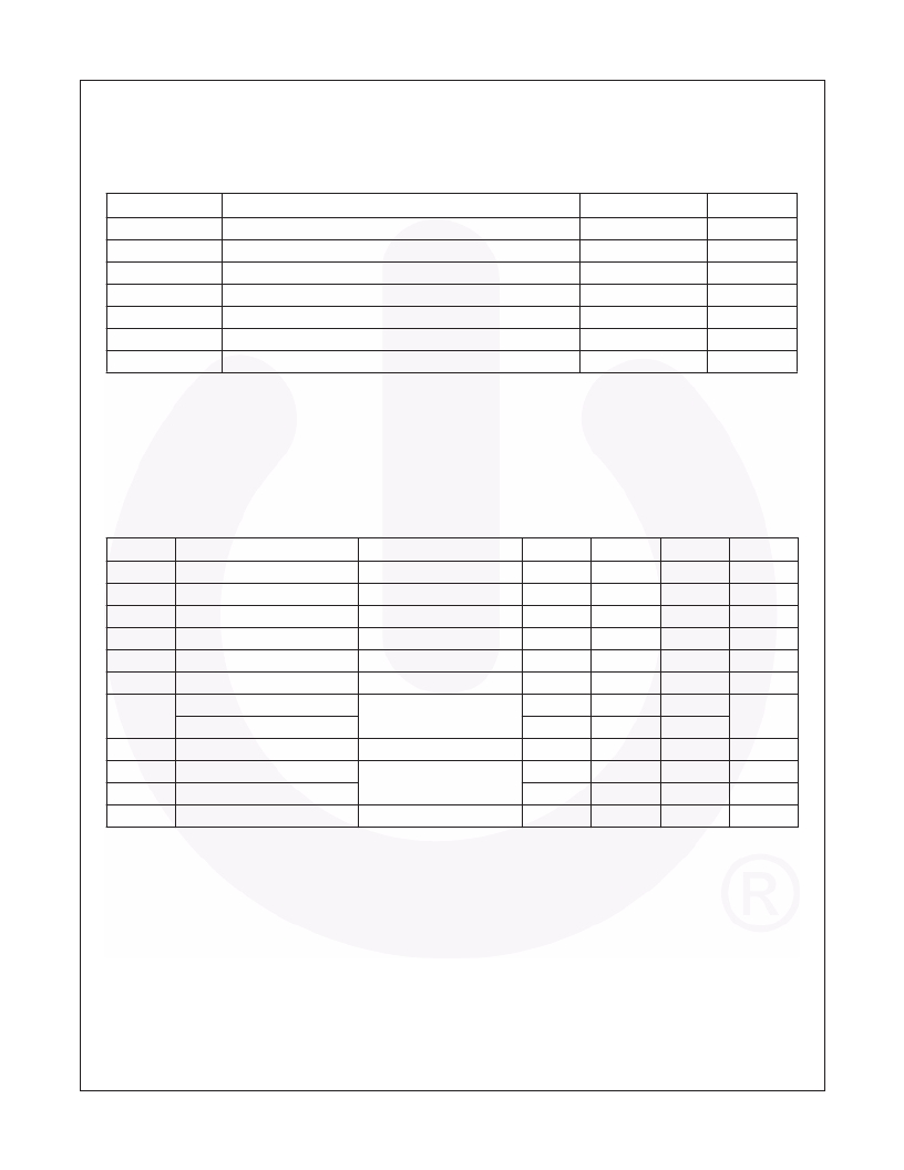
Absolute Maximum Ratings (T A = 25°C unless otherwise specified)
Stresses exceeding the absolute maximum ratings may damage the device. The device may not function or be
operable above the recommended operating conditions and stressing the parts to these levels is not recommended.
In addition, extended exposure to stresses above the recommended operating conditions may affect device reliability.
The absolute maximum ratings are stress ratings only.
Symbol
T OPR
T STG
T SOL-I
Parameter
Operating Temperature
Storage Temperature
Soldering Temperature (Iron) (2)(3)(4)
Rating
-40 to +100
-40 to +100
240 for 5 sec
Units
°C
°C
°C
T SOL-F
Soldering Temperature
(Flow) (2)(3)
260 for 10 sec
°C
I F
V R
P D
Continuous Forward Current
Reverse Voltage
Power Dissipation (1)
100
5
100
mA
V
mW
Notes:
1. Derate power dissipation linearly 2.67mW/°C above 25°C.
2. RMA flux is recommended.
3. Methanol or isopropyl alcohols are recommended as cleaning agents.
4. Soldering iron 1/16" (1.6mm) minimum from housing.
Electrical / Optical Characteristics (T A = 25°C)
Symbol
λ PE
Parameter
Peak Emission Wavelength
Test Conditions
I F = 20mA
Min.
Typ.
890
Max.
Units
nm
TC λ
Temperature Coef?cient
0.2
nm / °C
2 Θ 1 /2
V F
TC VF
I R
Emission Angle
Forward Voltage
Temperature Coef?cient
Reverse Current
I F = 100mA
I F = 100mA, tp = 20ms
V R = 5V
50
-6
1.7
10
°
V
mV / °C
μA
I E
Radiant Intensity QEE122
I F = 100mA, tp = 20ms
4
9
16
mW/sr
Radiant Intensity QEE123
8
9
TC IE
Temperature Coef?cient
-0.3
% / °C
t r
t f
C j
Rise Time
Fall Time
Junction Capacitance
I F = 100mA
V R = 0V
900
800
11
ns
ns
pF
?2004 Fairchild Semiconductor Corporation
QEE122, QEE123 Rev. 1.0.0
2
www.fairchildsemi.com
发布紧急采购,3分钟左右您将得到回复。
相关PDF资料
QEE273
LED EMITTER IR SIDELOOKER
QFM-TRX1-24G
TRANSCEIVER MOD RF 2.4GHZ 3.6V
QHX220IQSR
IC RF NOISE CANCELLING 16QFN
QRD1113
SENSR OPTO TRANS 1.27MM REFL PCB
QRE1113GR
SENSOR OPTO TRANS REFL SMD PHOTO
QRM85BXXG02E
LED PMI REAR MOUNT GREEN
QS5K2TR
MOSFET 2N-CH 30V 2A TSMT5
QS5U12TR
MOSFET N-CH 30V 2A TSMT5
相关代理商/技术参数
QEE123K
制造商:Rochester Electronics LLC 功能描述:- Bulk
QEE123K.E3R0
制造商:Rochester Electronics LLC 功能描述:- Bulk
QEE123K_E3R0
功能描述:光电晶体管 0.4mW 1.7V IR LED RoHS:否 制造商:OSRAM Opto Semiconductors 最大功率耗散:165 mW 最大暗电流:200 nA 封装 / 箱体:T-1
QEE213
功能描述:红外发射源 GaaS Type a LED Sidelooker RoHS:否 制造商:Fairchild Semiconductor 波长:880 nm 射束角:+/- 25 辐射强度: 最大工作温度:+ 100 C 最小工作温度:- 40 C 封装 / 箱体:Side Looker 封装:Bulk
QEE213_05
制造商:FAIRCHILD 制造商全称:Fairchild Semiconductor 功能描述:Plastic Infrared Light Emitting Diode
QEE213_Q
功能描述:红外发射源 GaaS Type a LED Sidelooker
RoHS:否 制造商:Fairchild Semiconductor 波长:880 nm 射束角:+/- 25 辐射强度: 最大工作温度:+ 100 C 最小工作温度:- 40 C 封装 / 箱体:Side Looker 封装:Bulk
QEE273
功能描述:红外发射源 LED-IR SIDELOOKER USED IN QVE00130 RoHS:否 制造商:Fairchild Semiconductor 波长:880 nm 射束角:+/- 25 辐射强度: 最大工作温度:+ 100 C 最小工作温度:- 40 C 封装 / 箱体:Side Looker 封装:Bulk
QEE323
功能描述:红外发射源 LED FOR QRD SWT RECT PKG RoHS:否 制造商:Fairchild Semiconductor 波长:880 nm 射束角:+/- 25 辐射强度: 最大工作温度:+ 100 C 最小工作温度:- 40 C 封装 / 箱体:Side Looker 封装:Bulk
